Diamond is hard and transparent and is also a good insulator. The graphite, by contrast, is soft and dark and easy to conduct electricity. These two seemingly distant substances are actually composed of the same atom, i.e. carbon. The reason why they have completely different physical properties is that their atomic arrangement, i.e., the so-called lattice structure, is different. In nature, the difference is caused by different growth environment and conditions. So, can we artificially adjust the distance and arrangement of atoms to deform the lattice structure so as to change, or even to create, new physical properties?
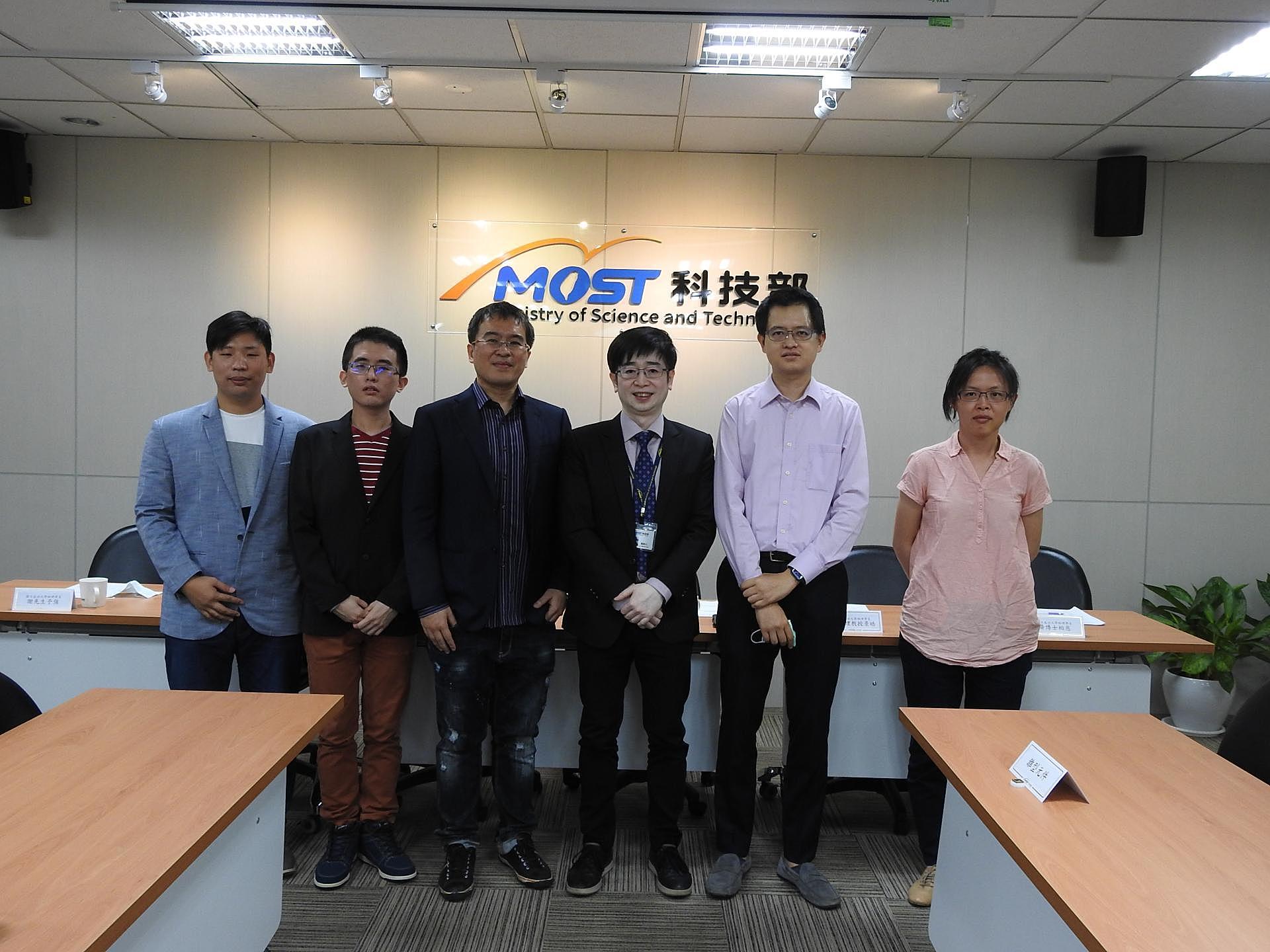
With the long-term support from the Ministry of Science and Technology (MOST) and the Higher Education Sprout Project at the National Cheng Kung University (NCKU), a joint research team led by Professor Ching-Hao Chang and Professor Tse-Ming Chen at the Department of Physics and the Center for Quantum Frontiers of Research & Technology (QFort) has successfully developed new techniques to achieve the artificial lattice deformation via patterned strain engineering in two-dimensional (2D) materials. They use this means to bring bilayer graphene into an exotic quantum state and demonstrate novel quantum electronics properties, with implications in future quantum technologies. This research work was published in the premier research journal "Nature Electronics" in February 2021.
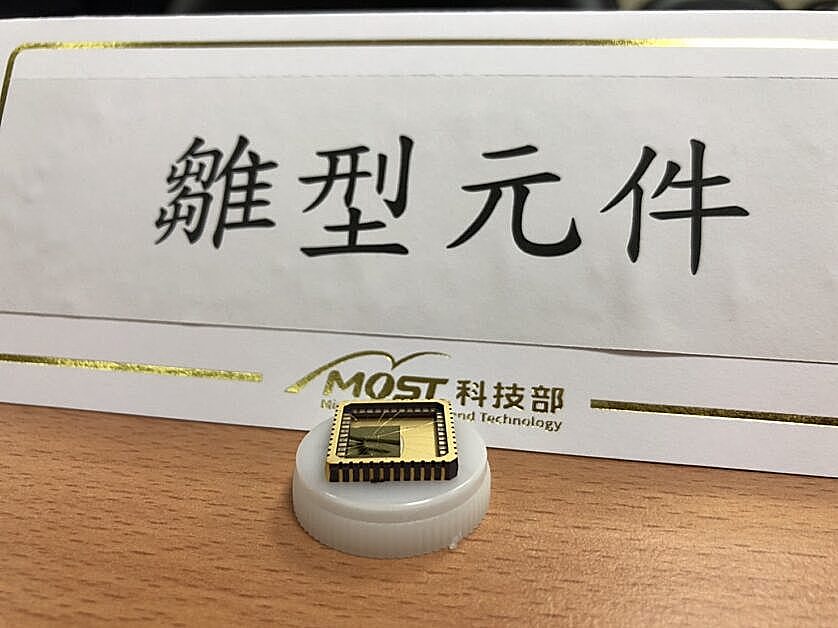
In recent years, research scientists and engineers are crazy about building nanoscale constructions by stacking layers and layers of graphene (or other atomic thin 2D materials) on top of each other, one by one, like playing with the LEGO building blocks. By twisting these atomic LEGO blocks with the formation of moiré pattern – a phenomenon that is commonly seen in our daily life – physicists was able to modulate the lattice structure (or more specifically, create a superlattice) and hence the electronic properties, transforming graphene from a zero-gap semiconductor to a superconductor, an insulator, or turning it into a ferromagnetism. This concept looks simple and, of course, very beautiful. However, due to the need to stack 2D materials that are as thin as a single atomic layer at a specific and precise angle, it is actually very challenging and pose difficulties for future industrial applications from the technological perspective. Dr. Sheng-Chin Ho, the first author of this work, and Prof. Tse-Ming Chen tried to ‘Think Different’: can we artificially and easily create a superlattice or structure in which the lattice has been distorted and/or misorientated to achieve a similar goal, or even something better?
Driven by this motivation, they came up with an idea and a device design, to artificially create the superlattice in bilayer graphene via nanofabrication. The research team develops new techniques to etch the surface of hexagonal boron nitride (hBN) substrates, then enabling the graphene placed upon it to conform to the surface topography and be lattice deformed accordingly. With these techniques, the substrate topography can be arbitrarily defined via nanolithography with the potential to approach 2.5D and 3D patterning, thereby opening up more possibilities.
In addition to the experimental realizations, Prof. Ching-Hao Chang, who is also the first author of this paper and a receipt of the Yushan Young Scholar Award, has developed the theory and performed the calculations with assistance from his colleagues to lay down the foundation for this research work. The theory completes the last piece of the puzzle, demonstrating the existence of two novel Hall effects at zero magnetic fields (or more accurately, without breaking time-reversal symmetry). For nearly 140 years since the discovery of the classical Hall effect, the magnetic field is generally considered to be a necessary condition for the Hall effect, or more accurately, a nonzero Hall conductivity. And these two Hall effects challenge this general belief. In addition to opening a new avenue for fundamental research into quantum geometrical and topological phenomena, their approach to band engineering will also be of great help to the future applications in 2D materials and quantum electronics.
With the support of the Ministry of Science and Technology, National Cheng Kung University has been very active in fundamental research in recent years, being the cornerstone for Taiwan's technological innovation and development. This kind of spirit casts the light of knowledge and gives birth to the QFort. Apart from the devotement to the research and development, QFort has also made great efforts in cultivating outstanding talents for Taiwan; for example, Dr. Sheng-Chin Ho, who led this breakthrough, has now been recruited to Harvard University as a postdoctoral researcher. All these have made the quantum technology research and development in Taiwan more competitive and integrated with the global network.
Source: Ministry of Science and Technology